

|
| Brand Name: | KAZ Circuit |
| Model Number: | PCB-B-041931 |
| MOQ: | 1 pc |
| Price: | USD/pc |
| Payment Terms: | T/T, Western Union, Paypal |
| Supply Ability: | 20,000 Square Meters / Month |
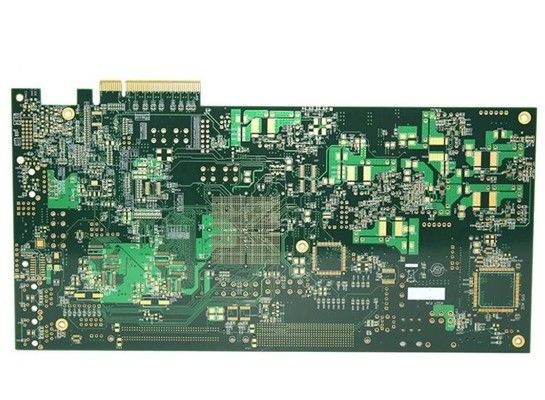
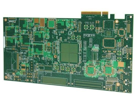
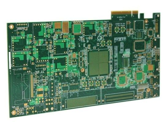
10 layers FR4 ENIG PCB Circuit Board Manufacturing with golden finger
Detail Specifications:
| Layers | 10 |
| Material | FR-4 |
| Board Thickness | 1.6mm |
| Copper Thickness | 1oz |
| Surface Treatment | HASL |
| Soldmask & Silkscreen | Green & White |
| Quality Standard | IPC Class 2, 100% E-testing |
| Certificates | TS16949, ISO9001, UL, RoHS |
What KAZ Circuit can do for you:
To get a full quotation of the PCB/PCBA, pls provide the information as below:
Company Informaiton:
KAZ Circuit is a professional PCB manufacturer from China since 2007, also provide PCB Assembly service for our customers. Now with about 300 employees. Certified with ISO9001,TS16949, UL, RoHS. We are confident to provide you quality products with factory-directed price within the fastest delivery time!
Manufacturer Capacity:
| Capacity | Double Sided: 12000 sq.m / month Multilayers: 8000sq.m / month |
| Min Line Width/Gap | 4/4 mil (1mil=0.0254mm) |
| Board Thickness | 0.3~4.0mm |
| Layers | 1~20 layers |
| Material | FR-4, Aluminum, PI |
| Copper Thickness | 0.5~4oz |
| Material Tg | Tg140~Tg170 |
| Max PCB Size | 600*1200mm |
| Min Hole Size | 0.2mm (+/- 0.025) |
| Surface Treatment | HASL, ENIG, OSP |
SMT Capacity
![]()
Multilayer PCB is a printed circuit board made of more than two layers of copper foil. It consists of an inner copper foil, an insulating substrate and an outer copper foil, and the interconnection between the layers is achieved by drilling and copper plating. Compared with single-layer or double-layer PCBs, multilayer PCBs can achieve higher wiring density and complex circuit design.
Advantages of multi-layer PCBs:
Higher wiring density and complex circuit design capabilities
Better electromagnetic compatibility and signal integrity
Shorter signal transmission paths, improved circuit performance
Higher reliability and mechanical strength
More flexible power and ground distribution
Composition of multi-layer PCBs:
Inner copper foil: Provides conductive layer and wiring
Insulating substrate (FR-4, high-frequency low-loss dielectric, etc.): Isolates and supports each copper foil layer
Outer copper foil: Provides surface wiring and interface
Perforated metallization: Realizes electrical connection between layers
Surface treatment: HASL, ENIG, OSP and other surface treatment processes
Design and manufacture of multi-layer PCBs:
Circuit design: Signal integrity, power/ground integrity design of multi-layer boards
Layout and wiring: Reasonable layer allocation and routing optimization
Process design: Aperture size, layer spacing, copper foil thickness, etc.
Manufacturing process: Lamination, drilling, copper plating, etching, surface treatment, etc.
More photoes of this 10 layers FR-4 ENIG High Tg PCB Circuit Board Manufacturing with golden finger
![]()
![]()
![]()

