

|
| Brand Name: | KAZ |
| Model Number: | KAZA-B-008 |
| MOQ: | 1 Unit |
| Price: | 0.1-20 USD / Unit |
| Payment Terms: | T/T, Western Union, MoneyGram, L/C, D/A |
| Supply Ability: | 2000 m2 / Month |
Customized electronic assembly Hasl 6 Layers pcb Optical&HDMI output RS232 Control usb pcba with CE&RoHS
1. Features of Pcba
1. One Stop OEM Service, Made in Shenzhen of China
2. Manufactured by Gerber File and BOM List from Customer
3. FR4 Material, Meet 94V0 standard
4. SMT, DIP technology suport
5. Lead Free HASL, Environmental Protection
6. UL, CE, ROHS Compliant
7. Shipping By DHL,UPS, TNT, EMS or Customer requirement
2. Specification of Pcba
| SMT | Position accuracy:20 um |
| Components size:0.4×0.2mm(01005) —130×79mm,Flip-CHIP,QFP,BGA,POP | |
| Max. component height::25mm | |
| Max. PCB size:680×500mm | |
| Min. PCB size:no limited | |
| PCB thickness:0.3 to 6mm | |
| PCB weight:3KG | |
| Wave-Solder | Max. PCB width:450mm |
| Min. PCB width: no limited | |
| Component height:Top 120mm/Bot 15mm | |
| Sweat-Solder | Metal type :part, whole, inlay, sidestep |
| Metal material:Copper , Aluminum | |
| Surface Finish:plating Au, plating sliver , plating Sn | |
| Air bladder rate:less than20% | |
| Press-fit | Press range:0-50KN |
| Max. PCB size:800X600mm | |
| Testing | ICT,Probe flying,burn-in,function test,temperature cycling |
Certifications:
ISO9001 / ISO14001 / ISO45001 (Military) / TS16949 (Automotive) / RoHS / UL
SMT PCB assembly refers to the process of manufacturing a printed circuit board (PCB) using surface mount technology, where electronic components are placed and soldered directly to the PCB surface rather than inserted through holes.
Key aspects of SMT PCB assembly include:
Component placement:
SMT components such as resistors, capacitors, integrated circuits (ICs) and other surface mount devices are placed directly on the PCB surface using automated pick and place machines.
Precise component placement is critical to ensure accurate alignment and reliable electrical connections.
Solder paste deposition:
Solder paste is a mixture of solder alloy particles and flux that is selectively deposited on the copper pads of a PCB using stencil printing or other automated processes.
Solder paste acts as an adhesive and conductive material that will form the electrical connection between the components and the PCB.
Reflow soldering:
After the components are placed, the PCB assembly goes through a reflow soldering process that heats the board in a controlled environment to melt the solder paste and form electrical and mechanical connections between the components and the PCB.
Reflow profiles including temperature, time and atmosphere are carefully optimized to ensure reliable solder joints.
Automatically detect:
After the reflow process, PCB assemblies are automatically inspected using a variety of techniques, such as optical inspection, X-ray inspection, or automated optical inspection (AOI).
These inspections help identify and correct any problems such as soldering defects, component misalignment or missing components.
Testing & Quality Control:
Comprehensive testing, including functional, electrical, and environmental testing, is performed to ensure that PCB assemblies meet required specifications and performance standards.
Implements quality control measures, such as statistical process control and failure analysis, to maintain high manufacturing standards and product reliability.
The advantages of SMT PCB assembly:
Higher Component Density: SMT components are smaller and can be placed closer together, resulting in a more compact, smaller PCB design.
Improved reliability: SMT solder joints are more resistant to vibration, shock and thermal cycling than through-hole connections.
Automated manufacturing: The SMT assembly process can be highly automated, increasing production efficiency and reducing manual labor.
Cost-Effectiveness: SMT assembly can be more cost-effective, especially for high-volume production, due to reduced material and labor costs.
SMT PCB assembly applications:
Consumer Electronics: Smartphones, Tablets, Laptops, and Other Portable Devices
Industrial electronics: control systems, automation equipment and power electronics equipment
Automotive electronics: engine control units, infotainment and safety systems
Aerospace and defense: avionics, satellite systems and military equipment
Medical devices: diagnostic equipment, implantable devices and portable healthcare solutions
SMT PCB assembly is a foundational technology used to produce compact, reliable, and cost-effective electronic devices in a variety of industries.
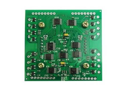
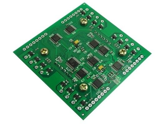
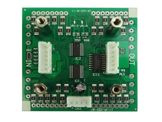
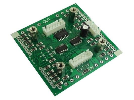
2. Pcba Pictures
![]()
![]()
![]()
![]()

