
|

| Brand Name: | KAZ |
| Model Number: | KAZA-B-045 |
| MOQ: | 1 Unit |
| Price: | 0.1-20 USD / Unit |
| Payment Terms: | T/T, Western Union, MoneyGram, L/C, D/A |
| Supply Ability: | 2000 m2 / Month |
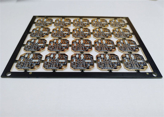
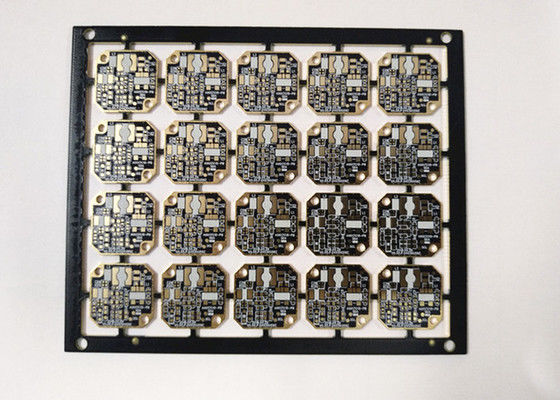
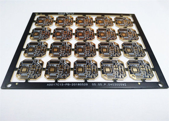
Gold Plating Surface Finishing Electronic Board Assembly Multilayer Circuit Board
Features of Circuit Board
1. One Stop OEM Service, Made in Shenzhen of China
2. Manufactured by Gerber File and BOM List from Customer
3. FR4 Material, Meet 94V0 standard
4. SMT, DIP technology suport
5. Lead Free HASL, Environmental Protection
6. UL, CE, ROHS Compliant
7. Shipping By DHL,UPS, TNT, EMS or Customer requirement
Circuit board Technical capability
| SMT | Position accuracy:20 um |
| Components size:0.4×0.2mm(01005) —130×79mm,Flip-CHIP,QFP,BGA,POP | |
| Max. component height::25mm | |
| Max. PCB size:680×500mm | |
| Min. PCB size:no limited | |
| PCB thickness:0.3 to 6mm | |
| PCB weight:3KG | |
| Wave-Solder | Max. PCB width:450mm |
| Min. PCB width: no limited | |
| Component height:Top 120mm/Bot 15mm | |
| Sweat-Solder | Metal type :part, whole, inlay, sidestep |
| Metal material:Copper , Aluminum | |
| Surface Finish:plating Au, plating sliver , plating Sn | |
| Air bladder rate:less than20% | |
| Press-fit | Press range:0-50KN |
| Max. PCB size:800X600mm | |
| Testing | ICT,Probe flying,burn-in,function test,temperature cycling |
Printed circuit boards (PCBs) are the basic components of electronic equipment and are the physical foundation that connects and supports various electronic components. It plays a vital role in the functionality and reliability of electronic systems.
Key aspects of electronic printed circuit boards include:
Layers and composition:
PCBs are typically made up of multiple layers, with the most common being a 2- or 4-layer design.
These layers are made of copper serving as conductive paths and a non-conductive substrate such as fiberglass (FR-4) or other specialty materials.
Other layers may include power and ground planes for power distribution and noise reduction.
Interconnects and Traces:
The copper layer is etched to form conductive traces that serve as pathways for electrical signals and power.
Vias are plated-through holes that connect traces between different layers, enabling multi-layer interconnections.
Trace width, spacing, and routing patterns are designed to optimize signal integrity, impedance, and overall electrical performance.
Electronic component:
Electronic components, such as integrated circuits, resistors, capacitors, and connectors, are mounted and soldered to the PCB.
The placement and routing of these components is critical to ensuring optimal performance, cooling, and overall system functionality.
PCB manufacturing technology:
PCB manufacturing processes typically involve steps such as lamination, drilling, copper plating, etching and solder mask application.
Advanced technologies such as laser drilling, advanced plating, and multi-layer co-lamination are used in specialized PCB designs.
PCB Assembly & Soldering:
Electronic components are placed and soldered onto the PCB either manually or automatically using techniques such as through-hole soldering or surface mount soldering.
Reflow soldering and wave soldering are common automated processes for connecting components.
Testing & Quality Control:
The PCB undergoes various testing and inspection processes such as visual inspection, electrical testing, and functional testing to ensure its reliability and performance.
Quality control measures, such as in-process inspections and design-for-manufacturability (DFM) practices, help maintain high standards in PCB production.
Electronic PCBs are used in a wide variety of applications, including consumer electronics, industrial equipment, automotive systems, medical devices, aerospace and telecommunications equipment, and more. Continuing advances in PCB technology, such as the development of high-density interconnect (HDI) PCBs and flexible PCBs, have enabled the creation of smaller, more powerful, and more energy-efficient electronic devices.
Circuit Board Pictures
![]()
![]()
![]()

