

|
| Brand Name: | KAZ |
| Model Number: | KAZA-B-007 |
| MOQ: | 1 Unit |
| Payment Terms: | T/T, Western Union, MoneyGram, L/C, D/A |
| Supply Ability: | 2000 m2 / Month |
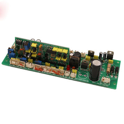
Electronic Circuit Board Assembly with contract manufacturing switch pcb assembly
Features of switch PCBA
Switch PCBA capability
| SMT | Position accuracy:20 um |
| Components size:0.4×0.2mm(01005) —130×79mm,Flip-CHIP,QFP,BGA,POP | |
| Max. component height::25mm | |
| Max. PCB size:680×500mm | |
| Min. PCB size:no limited | |
| PCB thickness:0.3 to 6mm | |
| PCB weight:3KG | |
| Wave-Solder | Max. PCB width:450mm |
| Min. PCB width: no limited | |
| Component height:Top 120mm/Bot 15mm | |
| Sweat-Solder | Metal type :part, whole, inlay, sidestep |
| Metal material:Copper , Aluminum | |
| Surface Finish:plating Au, plating sliver , plating Sn | |
| Air bladder rate:less than20% | |
| Press-fit | Press range:0-50KN |
| Max. PCB size:800X600mm | |
| Testing | ICT,Probe flying,burn-in,function test,temperature cycling |
Electronic circuit board assembly is the manufacturing process of assembling and interconnecting electronic components on printed circuit boards (PCBs) to create functional electronic devices.
The key steps in the electronic circuit board assembly process are:
PCB Manufacture:
PCBs are manufactured by layering and etching copper traces onto a non-conductive substrate such as fiberglass or other dielectric material.
PCB designs, including copper traces, component placement, and other features, are often created using computer-aided design (CAD) software.
Component purchasing:
Necessary electronic components, such as resistors, capacitors, integrated circuits (ICs), and connectors, are obtained from suppliers.
Select components carefully based on their electrical characteristics, physical size, and compatibility with the PCB design.
Element placement:
Electronic components are placed on the PCB using either manual or automated techniques such as pick and place machines.
Component placement is guided by the PCB design to ensure correct orientation and alignment on the board.
Soldering:
Components are fixed to the PCB and electrically connected through a soldering process.
This can be done using various methods, such as wave soldering, reflow soldering, or selective soldering.
The solder forms an electrically conductive and mechanical connection between the component leads and the PCB's copper pads.
Inspection and Testing:
The assembled PCB goes through visual inspection and various testing procedures to ensure the quality and functionality of the circuit.
These tests may include electrical testing, functional testing, environmental testing and reliability testing.
Any defects or issues discovered during the inspection and testing phase will be addressed before final assembly.
Cleaning and conformal coating:
After the soldering process, the PCB can be cleaned to remove any remaining flux or contaminants.
Depending on the application, a conformal coating may be applied to the PCB to provide environmental protection and improve reliability.
Final Assembly and Packaging:
Tested and inspected PCBs can be integrated into larger systems or enclosures, such as chassis, housings or other mechanical components.
The assembled products are then packaged and prepared for shipment or further distribution.
Electronic circuit board assembly is a critical process in the manufacturing of electronic devices, ensuring reliable and efficient operation of the final product. It combines technical expertise, precision manufacturing and quality control measures to provide high quality electronic systems.
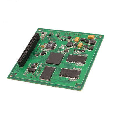
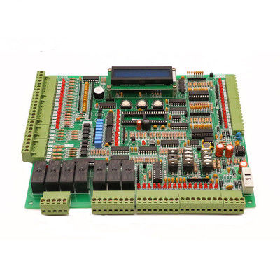
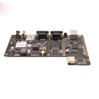
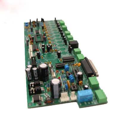
Switch PCBA Pictures
![]()
![]()
![]()
![]()
![]()

