

|
| Brand Name: | KAZpcb |
| Model Number: | PCB-B-039 |
| MOQ: | 1 |
| Price: | 0.1-3usd/pc |
| Payment Terms: | Paypal / , T/T, Western Union |
| Supply Ability: | 10000-20000square meters per month |
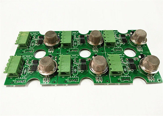
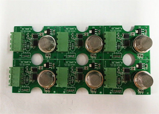
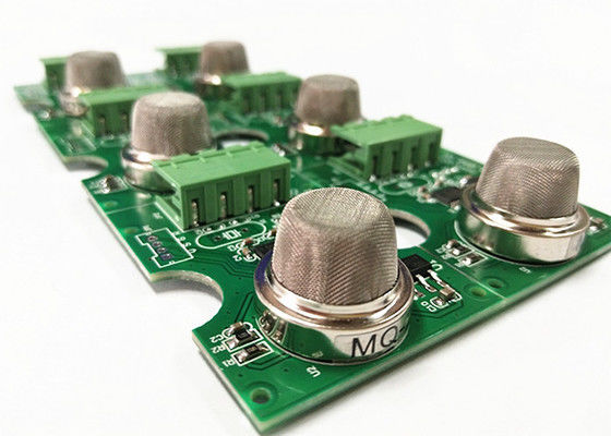
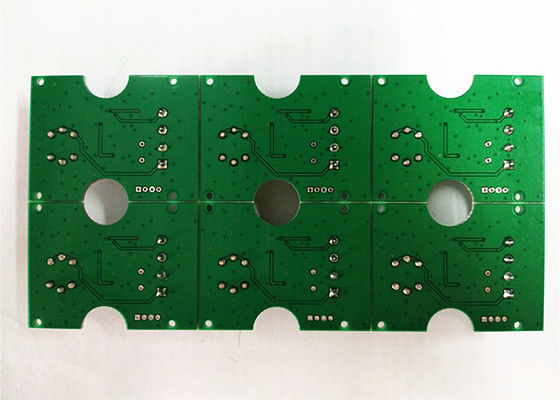
2-22 Layers FR4 Green Soldermask White Silkscreen Electronic Printed Circuit Boards Assembly
Introduction of FR4 Green soldermask White Silkscreen PCB Assembly with ENIG/OSP/ Gold Finger
| Categary | PCBA |
| Layer | 2-22L |
| Max Circuit Range | 1 – 2 sided 600 x 1000mm, Multilayer 600 x 600mm |
| Max Copper thickness | 12OZ |
| Min Line WidthGap | 3.54mil |
| Bare Board Test | Flying Probe |
| Plugging Vias Capability | 0.2-0.8mm |
| Solder Mask | Blue,White,Red,Green |
Brief introduction about Shenzhen KAZ Circuit Co,. Ltd.
Brief introduction
As a PCB and PCBA custom-made producer, KAZ Circuit Co., Ltd manufactures high precision single, double-sided, multilayer printed circuit board and metal substrate circuit board.
We manufacture pcb produsts depending on what you need and the gerber files you offered.
Manufacturer Capacity:
| Capacity | Double Sided: 12000 sq.m / month Multilayers: 8000sq.m / month |
| Min Line Width/Gap | 4/4 mil (1mil=0.0254mm) |
| Board Thickness | 0.3~4.0mm |
| Layers | 1~20 layers |
| Material | FR-4, Aluminum, PI |
| Copper Thickness | 0.5~4oz |
| Material Tg | Tg140~Tg170 |
| Max PCB Size | 600*1200mm |
| Min Hole Size | 0.2mm (+/- 0.025) |
| Surface Treatment | HASL, ENIG, OSP |
The services we offer:
| Layer |
Lead Time (Expedited service) |
Lead Time (Sample) |
| 2L | 24h | 3-4days |
| 4L | 36h | 5-7days |
| 6L | 72h | 8-10days |
|
Notes |
Min drill hole: 0.2mm |
|
|
Application |
Industry Control, Communication, Security, LED lighting, Digital, Smart products ect. | |
|
Projects |
HDI Board, Gold Finger, High Frequency Board, Blind/buried multilayer board, SMT/DIP ect. | |
The customers we establish business relationship with:
![]()
Electronic circuit board assembly is the manufacturing process of assembling and interconnecting electronic components on printed circuit boards (PCBs) to create functional electronic devices.
The key steps in the electronic circuit board assembly process are:
PCB Manufacture:
PCBs are manufactured by layering and etching copper traces onto a non-conductive substrate such as fiberglass or other dielectric material.
PCB designs, including copper traces, component placement, and other features, are often created using computer-aided design (CAD) software.
Component purchasing:
Necessary electronic components, such as resistors, capacitors, integrated circuits (ICs), and connectors, are obtained from suppliers.
Select components carefully based on their electrical characteristics, physical size, and compatibility with the PCB design.
Element placement:
Electronic components are placed on the PCB using either manual or automated techniques such as pick and place machines.
Component placement is guided by the PCB design to ensure correct orientation and alignment on the board.
Soldering:
Components are fixed to the PCB and electrically connected through a soldering process.
This can be done using various methods, such as wave soldering, reflow soldering, or selective soldering.
The solder forms an electrically conductive and mechanical connection between the component leads and the PCB's copper pads.
Inspection and Testing:
The assembled PCB goes through visual inspection and various testing procedures to ensure the quality and functionality of the circuit.
These tests may include electrical testing, functional testing, environmental testing and reliability testing.
Any defects or issues discovered during the inspection and testing phase will be addressed before final assembly.
Cleaning and conformal coating:
After the soldering process, the PCB can be cleaned to remove any remaining flux or contaminants.
Depending on the application, a conformal coating may be applied to the PCB to provide environmental protection and improve reliability.
Final Assembly and Packaging:
Tested and inspected PCBs can be integrated into larger systems or enclosures, such as chassis, housings or other mechanical components.
The assembled products are then packaged and prepared for shipment or further distribution.
Electronic circuit board assembly is a critical process in the manufacturing of electronic devices, ensuring reliable and efficient operation of the final product. It combines technical expertise, precision manufacturing and quality control measures to provide high quality electronic systems.
More pictures of FR4 Green soldermask White Silkscreen PCB Assembly with ENIG/OSP/ Gold Finger
![]()
![]()
![]()
![]()
May I know if there is any project requiring pcb or pcba products that we could help to quote?

