

|
| Brand Name: | Null |
| Model Number: | KAZ |
| MOQ: | 1pcs |
| Price: | 0.1-5 USD |
| Payment Terms: | T/T, Western Union, Paypal |
| Supply Ability: | 20000 meter |
8 Layer HDI pcb factory pcb assembly shenzhen printed circuit board manufacturers
1. Detailed Specifications
| Material | FR4 |
| Board Thickness | 1.6mm |
| Surface Treatment | ENIG 2U'' |
| Copper Thickness | 1/1/1/1/1/1/1/1 OZ |
| Soldermask | Green |
| Silkscreen | White |
| The Min Laser Drill Hole | 4 Mill |
| Panel | V-Cut |
Introduction:
Printed Circuit Board Assembly it to plug the SMT(Surface Mounted Technolofy) and the DIP in the Printed Circuit Board, also called PCBA.
Production:
Both SMT and DIP are means of integrating components in the PCB board. The main difference is that SMT does not need to drill holes on the PCB,while it's nacessary for the DIP to plug the pin of the component into the drilled hole.
SMT:
Mainly use the paste to pack machine to attach some micro components the PCB board. The production process is as follows: the PCB board positioning, solder paste printing, paste and pack, return to the soldering stove, finally inspection.
Printed Circuit Board (PCB) assembly, also known as circuit board assembly or PCB manufacturing, is the process of populating and soldering electronic components onto a PCB to create a functional electronic device. The PCB assembly process typically involves the following steps:
Components Procurement: The first step is to source and procure the electronic components required for the PCB assembly. These components can include resistors, capacitors, integrated circuits, connectors, and more. The components can be sourced from various suppliers or distributors.
PCB Fabrication: Before assembly, the PCB itself needs to be fabricated. This involves designing the PCB layout, creating the PCB design files, manufacturing the bare PCB, and applying the necessary copper traces, solder mask, and silkscreen markings. PCB fabrication can be done using different techniques such as etching, milling, or printing.
Component Placement: In this step, the electronic components are mounted on the PCB. The two primary methods of component placement are surface mount technology (SMT) and through-hole technology (THT). SMT components are placed on the surface of the PCB and soldered using solder paste and reflow soldering techniques. THT components have leads that pass through holes in the PCB and are soldered on the opposite side.
Soldering: Once the components are placed on the PCB, the soldering process is performed to create electrical and mechanical connections. Soldering can be done through various methods such as reflow soldering (for SMT components), wave soldering (for THT components), or manual soldering (for specific components or rework).
Inspection and Testing: After soldering, the assembled PCB undergoes inspection and testing to ensure the quality and functionality of the electronic device. Automated optical inspection (AOI), X-ray inspection, functional testing, and other methods may be employed to identify any defects or faults.
Final Assembly: Once the PCB assembly is verified to be functioning correctly, it can be further integrated into the final product assembly. This may involve additional mechanical assembly, enclosure installation, and connection to other subsystems or components.
The PCB assembly process may vary depending on the specific requirements, industry standards, and manufacturing capabilities of the contract manufacturer or assembly house. Additionally, advanced techniques such as selective soldering, conformal coating application, and testing procedures may be employed based on the complexity and functionality of the electronic device being assembled.
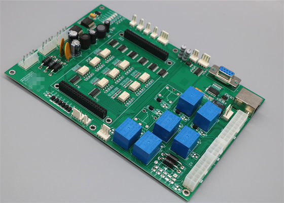
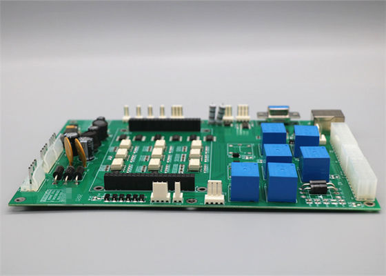
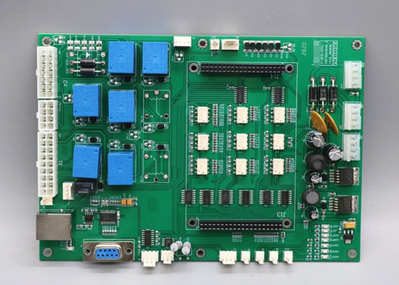
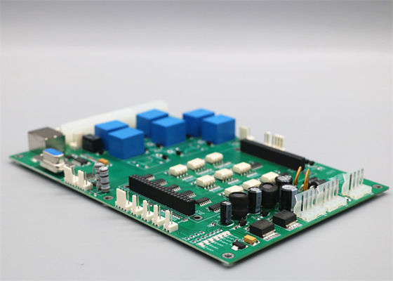
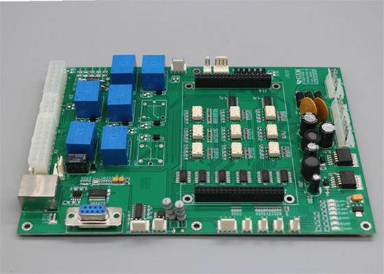
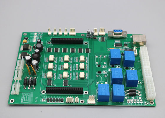
2. Pictures ![]()
![]()
![]()
![]()
![]()
![]()
![]()
FAQ
Q: What files do you use in PCB fabrication?
A: Gerber or Eagle, BOM listing, PNP and Components Position
Q:Is it possible you could offer sample?
A: Yes, we can custom you sample to test before mass production
Q: When will I get the quotation after sent Gerber, BOM and test procedure?
A: Within 6 hours for PCB quotation and around 24-48 hours for PCBA quotation.
Q: How can I know the process of my PCB production?
A: 5-7days for PCB production and components purchasing, and 14 days for PCB assembly and Testing.
Q: How can I make sure the quality of my PCB?
A: We ensure that each piece of PCB products work well before shipping. We'll test all of them according to your test procedure.

